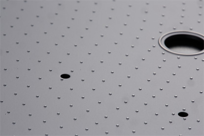
Vacuum chuck
We can provide optimal pin chucks tailored to strict customer requirements through customized design using world-class flattening process technology.
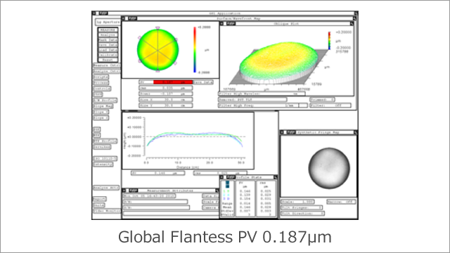
Seeking to achieve ultimate flatness, we have realized a flatness of 0.2 μm for 12-inch chucks. We can flexibly adjust planar shapes of pin chucks with variable unevenness according to the shapes of wafers and customize absorption zones and pin patterns to enhance absorption responsiveness.
Features/Usage
Features
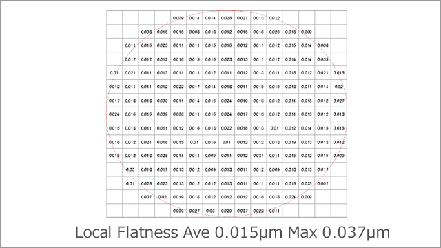
- High precision: flatness of 0.2 μm with L/F of not more than 0.05 μm
- Shape control: adjustable chuck shapes in accordance with the shapes of wafers (unevenness control)
- Absorption responsiveness: customized planar design following specifications
Usage
- Wafer fixation for semiconductor exposure equipment
- Wafer fixation for wafer inspection equipment
Our Technologies
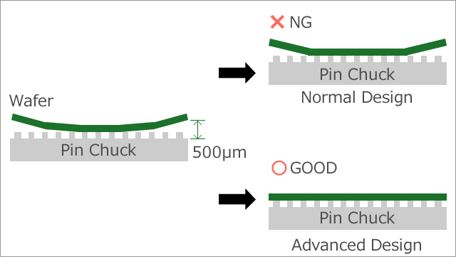
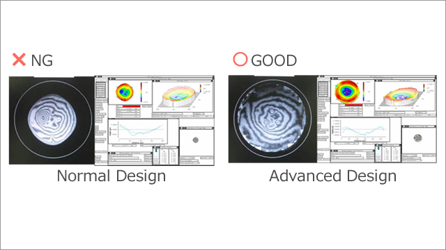
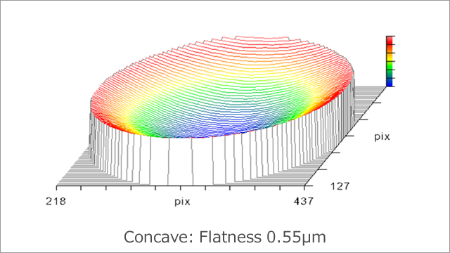
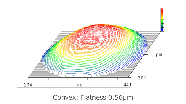
◆Absorption of warped wafers
Realization of ideal absorption using optimized absorption zones and pin arrangement
◆Precise flatness for 12-inch chucks
Flatness of 0.2 μm with L/F of not more than 0.05 μm
◆Shape control
Flexible chuck shapes according to the shapes of wafers (unevenness control)
Download Catalog
Inquiry

Contact us anytime.:


Request product specifications, information or quotes.